


SINGAPORE – To meet the surging global demand for advanced chips used in AI applications, Singapore semiconductor companies are rapidly expanding their presence in the US, adding facilities and boosting manpower.
Advanced semiconductor packaging firm Ecsal Technologies is eyeing a new US facility and expects to double its headcount in the United States by the end of 2026.
It comes as the Singapore company seeks to capitalise on the AI boom, which has emerged as a significant driver of investment and economic growth in the US.
The company is moving quickly to stay competitive in the AI race, such as by speeding up its product development cycle, Ecsal Technologies managing director Edmund Chua told The Straits Times.
“We used to renew a product or model every two years. Now we are looking at refreshing them once every six months due to the shortening of the semiconductor cycle,” he said, referring to the accelerated pace of innovation in the industry.
The company currently operates a service support base in Arizona to serve clients there and in other US states, with plans to expand to Texas to be closer to its customers.
Firms like Ecsal Technologies are critical to the semiconductor ecosystem, supplying equipment used in the packaging of advanced processors and memory chips.
The US semiconductor industry remains the global leader, accounting for just over half of global semiconductor sales revenue, according to a 2025 Semiconductor Industry Association report.
Other Singapore semiconductor firms are also expanding in the US to tap growing demand driven by generative artificial intelligence and high-performance computing.
Since setting up shop in El Dorado Hills in November 2025, wafer defect inspection systems provider Industrial Vision Technology (Visiontec) has been receiving strong interest from potential customers.
“At the moment, customers send their wafers to Singapore because we do not yet have a testing platform in the US,” said Visiontec’s US general manager Howard Sin.
Wafers are the physical foundation on which semiconductor chips are built.
Sin said that setting up a US-based testing platform is a key priority. The firm is considering California, New Jersey or North Carolina for their proximity to major clients and research institutions.
Visiontec is also engaging with US chipmakers including Wolfspeed, which develops and manufactures semiconductor technologies based on silicon carbide for power electronics applications.
Visiontec aims to grow its US team to five employees by the end of 2027, and double that to 10 by 2029.

Howard Sin, US general manager of Visiontec.
PHOTO: VISIONTEC
Sin said there is strong demand for high-quality, high-performance wafer defect inspection systems as the AI boom fuels the need for more advanced chips, for which even minor defects can affect performance and yield.
“We are riding this wave of AI and its energy needs. AI needs compute, data and power – power is the most formidable pillar. There’s a need for these systems to run on very high-efficiency, high-reliability chips,” he added in a Zoom interview from El Dorado Hills, where the firm’s US business development office is based.
The area was chosen for its proximity to Silicon Valley – a 2½-hour drive away – giving Visiontec access to major technology firms such as Nvidia, Broadcom and Intel, as well as a broader ecosystem of AI and semiconductor companies, Sin said.
Similarly, semiconductor testing equipment maker AEM, which counts US chip giant Intel as a long-time customer, set up a sales office and R&D centre in Carlsbad, California, to be closer to its US clients.
This allows the firm to engage closely with the engineers, procurement teams and commercial leads at the hyperscalers, chip designers and foundries driving the AI build-out.
AEM chief of staff Samir Mowla said the company is hiring engineering talent in the US, as well as Singapore, France and South Korea, to meet rising demand for its solutions and keep up with customers’ fast rate of innovation. He did not specify the number of new hires planned.
Fuelled by strong demand for advanced AI chip testing solutions, AEM’s revenue grew to about $399 million in 2025, and it has guided revenue to reach $550 million to $600 million in 2026.
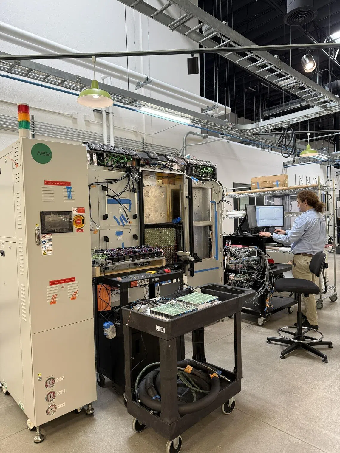
AEM’s US team is primarily customer-facing, covering application
engineering, technical support, sales and R&D.
PHOTO: ENTERPRISE SINGAPORE
Agentic AI, or AI agents that can complete tasks independently with limited human intervention, is a structural tailwind for AEM, said Mowla.
Simultaneously, the growing complexity of next-generation chip architectures is intensifying semiconductor test requirements – an area where AEM’s high-parallel test capabilities are well positioned, he added.
In semiconductor testing, high-parallel means the ability to test many chips simultaneously rather than one at a time.
Mowla said the company’s test solutions help customers cut their testing costs significantly by testing up to 80 high-power devices concurrently, ensuring precise, stable temperature control across all devices under testing, and letting customers tailor the process to their specific needs.
While the US market presents significant growth opportunities, Singapore semiconductor firms continue to grapple with challenges ranging from talent recruitment to higher operating costs.
Breaking into the market is no easy feat, said Visiontec’s Sin, but once a company establishes itself, those barriers can become a competitive advantage.
